
The combined measurement of the absorption and emission of a material allows access to information such as doping, homogeneity etc. They are usually obtained with purely optical techniques, which limits the achievable spatial resolution. Recent advances in transmission electron spectroscopy (STEM) offer new perspectives to quantify the optical properties of semiconductor monolayers with a resolution of the order of ten nanometers.
The spectral signatures of excitons and charged excitons in monolayers of transition metal dichalcogenides (TMDs) have been measured at the nanoscale in emission and absorption. To understand the origin of their variations, these measurements were correlated with deformation and This allowed to confirm that the emission of charged excitons is strongly influenced by their local dielectric environment. This work is published in the journal Nano Letters.
In this work, specific samples, consisting of WS2 monolayers encapsulated in hexagonal boron nitride (h-BN) deposited on an electron microscopy grid (Figure), were fabricated in collaboration with a team from the Massachusetts Institute of Technology (MIT). The physicists used the STEM developed at the Solid State Physics Laboratory (ChromaTEM, TEMPOS project), equipped with an electron monochromator allowing a resolution in EELS comparable to that of optical absorption measurements but with a nanometric resolution. One of the advantages of this device is to be able to combine both emission (cathodoluminescence) and absorption measurements by electron energy loss spectroscopy (EELS) with imaging techniques (sample morphology, deformation maps or chemical environment maps (Figure). In particular, TMDs monolayers show localized light emissions. Some of these emissions have been identified as single photon sources. The microscopic origin of these emissions is still unknown, and can be explored by making strain maps or atomically resolved images correlated to the cathodolumines-cence emission. Many systems can be characterized in this way in the future, which would allow access to information on the origin of these variations in optical phenomena at the nanometer scale.
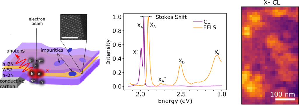
Figure. Left, schematic of the process leading to cathodoluminescence (CL) emission from the monolayer (orange) encapsulated in h-BN (purple). An atomically resolved image of the monolayer near an edge is visible (scale 2 nm). In the center, CL and EELS spectra are displayed, with the different excitonic peaks indicated. On the right, an intensity map of the cathodoluminescent loaded exciton is displayed. Lower intensity patterns (purple) were correlated with the presence of contami-nants.
Reference
Nanoscale modification of WS2 trion emission by its local electromagnetic environment
N. Bonnet, H. Y. Lee, F. Shao, S. Y. Woo, J. D. Blazit, K. Watanabe, T. Taniguchi, A. Zobelli, O. Stéphan, M. Kociak, S. Gradečak, L. H. G. Tizei
Nano Letters, 2021, 21, 10178-10185
doi: 10.1021/acs.nanolett.1c02600
Contacts
Noemie Bonnet
Luiz Galvao-Tizei