The LPS micro and nanotechnologies facility (platform) located at the basement of the SOUTH wing offers a large set of fabrication and characterization technologies. More than 250 m² are dedicated to thin films deposition, lithography techniques, transfer methods and samples characterization. Around 40 internal and 10 external users work on the platform. Three engineers and an assistant engineer manage the equipment and perform process (Micro and Nanotechnologies group SMNT).
- Thin film deposition
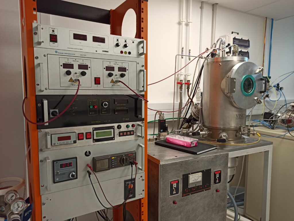
The platform include seven vacuum coating machines
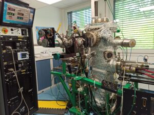
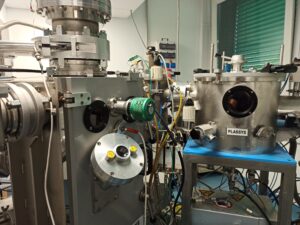
IDMAG: An ultra-high vacuum system with two e-beam gun is dedicated to magnetic films; this system can be used to study magnetic alloys or multilayer for instance. The equipment include two e-guns with seven materials (Al, V, Fe, Co, Ni, Cu, Pd, Ta, Au, Gd, Tb, NiFe, CoFe).
NS2: Two ultra-high vacuum e-beam systems are used to operate metallic and superconducting thin film deposition. One of them offers the possibility to deposit through metallic mask. This technique is useful to pattern devices without classical lithography techniques and the resolution is 10 µm. This two system included also oxidation to perform Josephson junctions for example. A homemade sputtering machine is dedicated to niobium deposition.
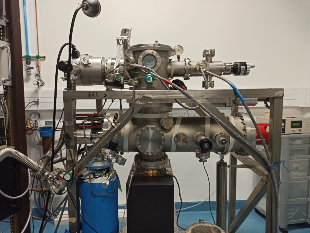
MESO: The group use a cluster with three systems including an e-beam gun chamber and a DC sputtering chamber for metallic films. The last chamber is dedicated to insulating layers made by RF sputtering. This cluster is used to perform ohmic or superconducting contacts on graphene or carbon nanotubes for example.
SUMAG: the group perform cuprate and iridate superconducting layer by RF sputtering.
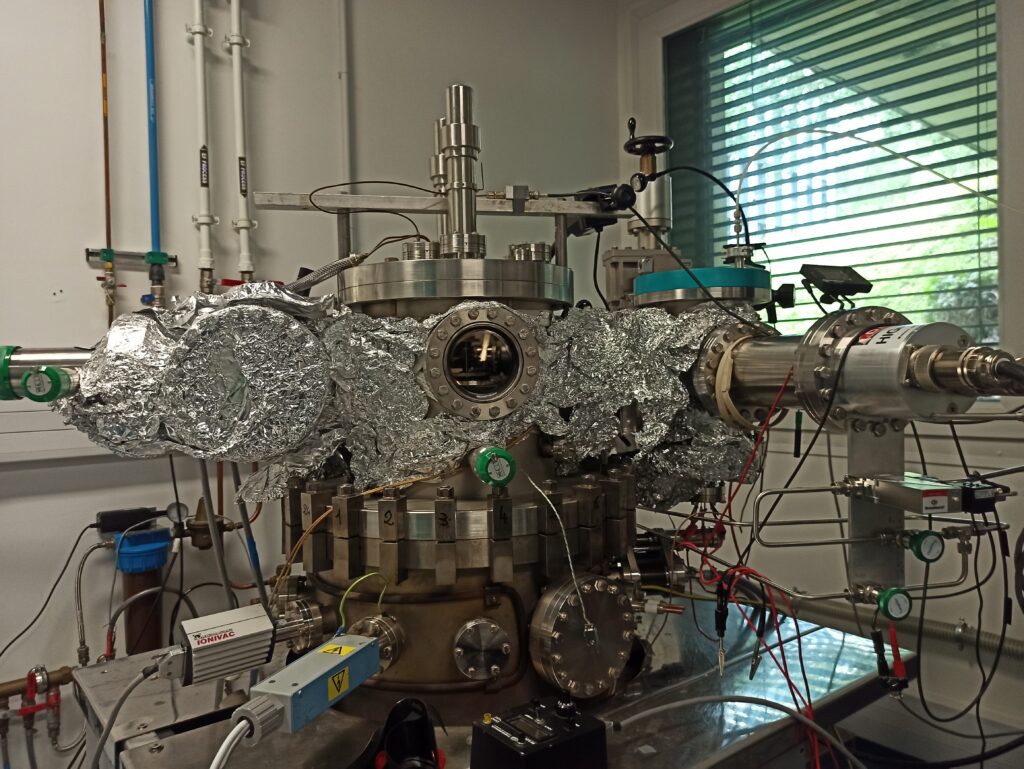
The last system is a two boats thermal evaporation system for metallic deposition managed only by the SMNT and opened to other groups or external users.
- Lithography systems
– For process with resolution over 2 µm we use an optical photolithographic system (Microwriter baby from DMO). It is a direct-write machine without chromium-glass mask, the mask is holding in software. The machine allows rapid prototyping compare to other techniques. We use it for fabrication of RF resonators, ohmic contacts, or surface texturing for example.
– For processing devices with resolution better than 2 µm we use a e-beam lithography system (NGPS) mounted on a scanning electron microscope (Zeiss Supra55VP). We achieve resolution better than 50 nm. Several teams of the laboratory involved in nanofabrication use it.
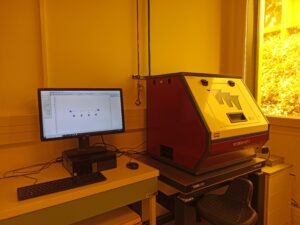
Direct writing lithography system DMO 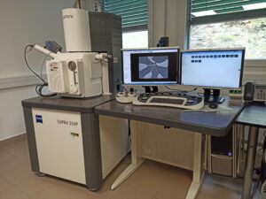
scanning electron microscope Zeiss Supra55VP
- Etching
– Ion Beam etching: Milling is achieved by directing a beam of particle (argon) at a substrate with a metallic mask made (aluminium for example). After milling the mask could be removed chemically.
-Reactive ion etching (RIE) uses chemically reactive plasma to remove material through a mask. The tool (ICP Cobra system from Oxford) is equipped with the following gases : SF6, C4F8, CF4, O2 and Ar. It is used to etch a wide range of materials : Si, SiO2, Nb, Ti…
In addition, optical emission spectroscopy (OES) is installed to enable endpoint detection. The system is loadlocked for sample entry and removal.
Ion Beam Etching 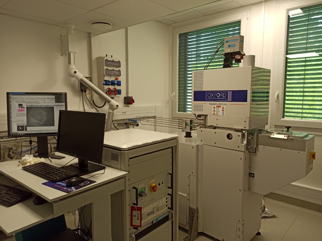
RIE ICP Oxford Cobra
- Characterization
Scanning electron microscopy and micro chemical analysis is also available. We perform these observations by using a field emission gun microscope, and an energy dispersive X-ray spectrometer. It offers high performances for observation (imaging resolution better than 2nm) especially for insulating sample studies (nano-devices on insulating substrate, biological samples…) due to its low voltage capabilities.
Others facilities for micro and nano processes are shared in a clean room. It concerns wafer cleaning by oxygen plasma, wafer cutting, micro wire bonding, probe station for electrical checking, optical microscopes, mechanical profilometer, fume hood for chemical steps, and spin coating.
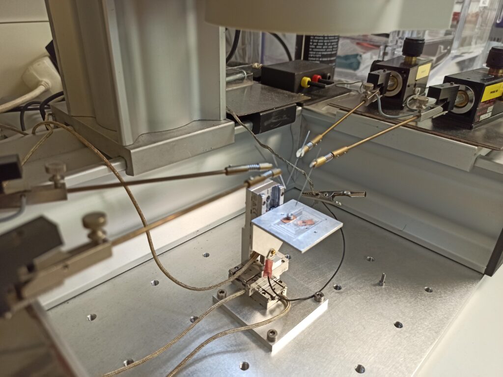
Probe Station 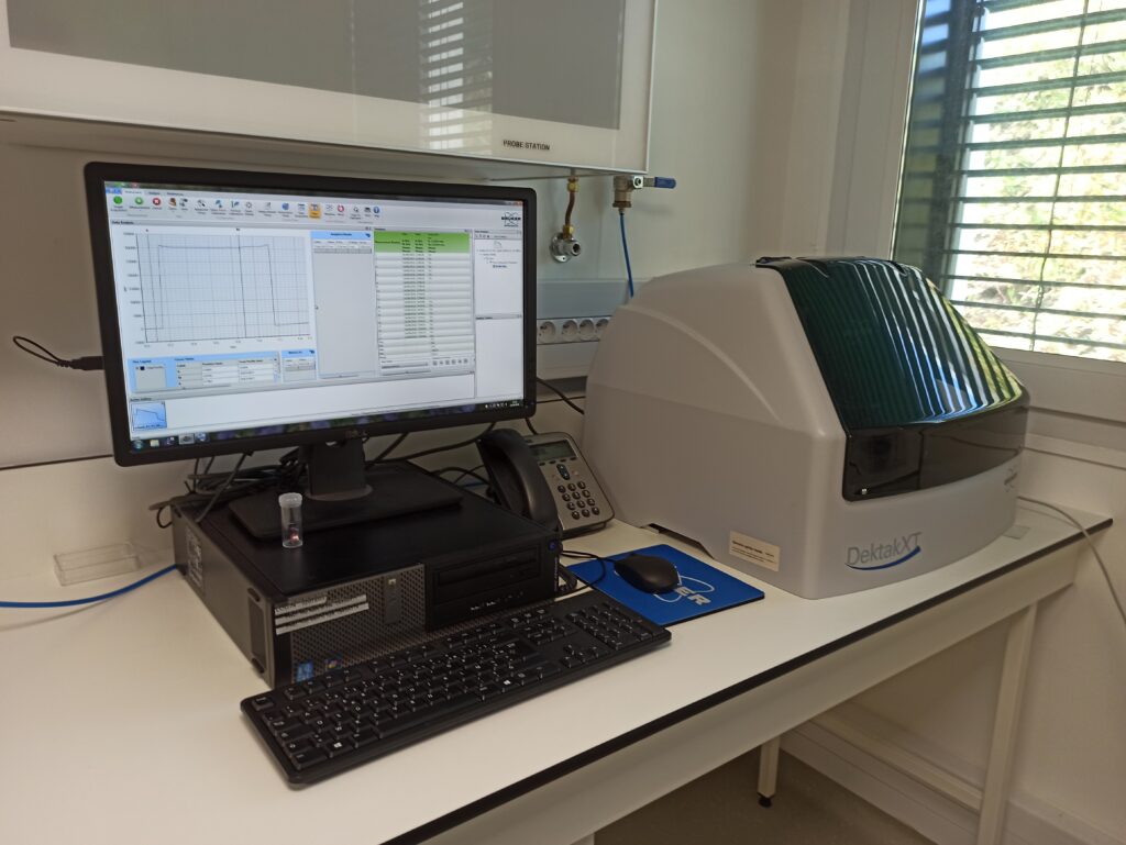
Profilometer Bruker DektakXT 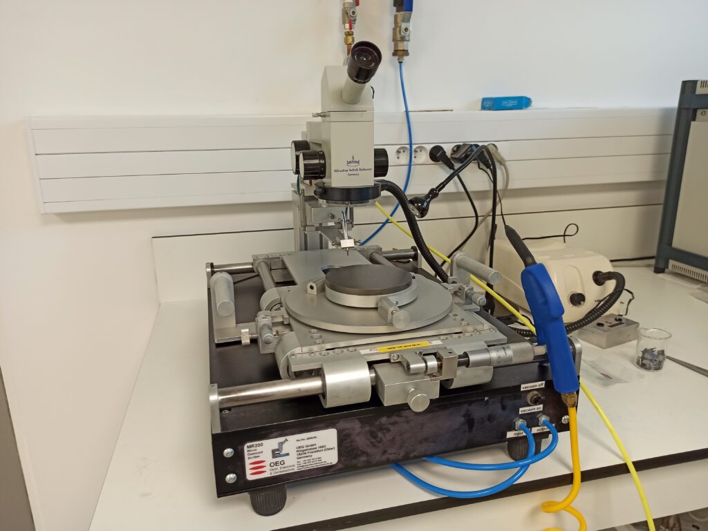
Scriber 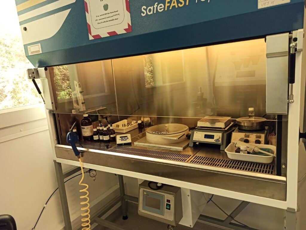
Spin Coater
The laboratory is strongly involved in the development of processes by focus ions beam. We share with two partners (C2N and SPEC) a helium and neon focus ion beam microscope called Zeiss Orion Nanofab. The machine is set up at Palaiseau (C2N). We perform observation, milling and deposition with one instrument. We started studies concerning junction texturing for plasmonic applications, or bismuth nanowire contacting by in situ deposition of tungsten.
Most facilities for micro and nano-fabrication and processes are shared. The equipment is also opened for external collaboration.