| Researchers and engineers at Laboratoire de Physique des Solides (a joint research unit of CNRS and Paris-Saclay University) have developed an innovative device capable of applying mechanical strain to two-dimensional materials at cryogenic temperatures, while simultaneously probing the 3D deformation of the atomic lattice in situ using X-ray diffraction, as well as the electronic transport properties. Using this device, they observed a novel behavior of correlated electrons aligning along the direction of mechanical strain, a behavior directly linked to the change in symmetry of the atomic structure. They also demonstrated that the transition temperature to this state increases remarkably by over 30 degrees, opening up new possibilities for manipulating electronic states in 2D systems through mechanical strain. |
Two-dimensional (2D) materials have garnered significant attention due to their unique electronic properties stemming from quantum effects, offering numerous potential applications. Unlike three-dimensional materials, 2D materials allow for flexible control of their properties through mechanical, electronic, optical, and magnetic excitations. Their layered structure, consisting of weakly bonded atomic planes, leads to anisotropic properties, which notably influence electronic conduction. Some of these materials exhibit superconductivity, while others have semiconductor or optoelectronic characteristics, paving the way for applications in electronics and photovoltaics. However, the connection between atomic ordering within these materials and the electronic properties they exhibit is not always well understood, yet it is crucial for achieving precise control over electronic properties through modifications to atomic structure.
To address this challenge, researchers and engineers at the Laboratoire de Physique des Solides have developed a one-of-a-kind biaxial strain device capable of applying mechanical deformations to 2D compounds across a wide temperature range (from -250°C to +100°C). This device is designed to be compatible with in-situ measurements that monitor atomic deformations in the structure (via X-ray diffraction – XRD) as well as electronic properties (through electronic transport measurements) during the deformation process. To highlight the link between atomic structure and electronic properties, researchers at the LPS, in collaboration with the Pprime Institute in Poitiers and the Néel Institute in Grenoble, studied a 2D material, TbTe₃, which exhibits particularly remarkable intrinsic properties
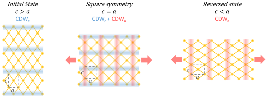
In its ground state, this system consists of a stack of weakly bonded 2D planes along the stacking direction (Van der Waals bonds). These planes exhibit an almost (but not quite!) square structure, with only a 0.2% difference between the lengths of the two sides, a and c, with c being slightly longer than a. However, from the perspective of electronic properties, electrons behave very differently depending on the main in-plane directions. At room temperature, the electron density is spatially modulated along the c direction, where atoms are more widely spaced, but not along the perpendicular a direction. This modulated phase is known as a Charge Density Wave (CDW).
Using the developed biaxial stretching device, the researchers in the consortium were able to alter the atomic structure within the planes, first giving it a square geometry (where a=c) by applying stretching along a, and then creating a rectangular geometry with an inversion in anisotropy direction (where a>c). By combining X-ray diffraction (XRD) measurements with electronic transport measurements, they observed that the orientation of the CDW modulation shifted progressively to align with the direction of the applied stretch, with both orientations coexisting when a=c. This work demonstrates that the symmetry of the atomic structure within the planes has a direct impact on the symmetry of the electronic properties.

Furthermore, they observed that the temperature at which the CDW appears increases by more than 30 degrees under mechanical deformation, while the amplitude of the CDWs formed under tension remains perfectly stable. This finding challenges current theoretical models regarding CDWs. This significant increase in the transition temperature opens up very promising avenues for studying other electronic phases in 2D systems, particularly superconductivity.
This innovative methodology represents a significant advancement in the exploration of electronic ordering phenomena that coexist or compete within condensed matter. By allowing for precise manipulation of atomic structure and modulation of electronic properties at the microscopic scale, it offers a novel perspective for probing the underlying mechanisms of these complex phenomena. This promising approach thus opens up new avenues for the fundamental understanding of materials physics and for the development of innovative electronic and quantum devices.
This research work has been published in the scientific journal “Nature Communications.”
Contributors
A. Gallo-Frantz, A. A. Sinchenko, D. Ghoneim, L. Ortega, D. Le Bolloc’h, V.L.R. Jacques (Équipe LUTECE, Laboratoire de Physique des Solides, UMR8502 Université Paris-Saclay, CNRS)
P. Godard, P.-O. Renault (Institut Pprime, CNRS-Université de Poitiers-ENSMA, 86962, Futuroscope-Chasseneuil Cedex, France)
A. Hadj-Azzem, J. E. Lorenzo, P. Monceau (Univ. Grenoble Alpes, CNRS, Grenoble INP, Institut Néel, 38000, Grenoble, France)
P.D. Grigoriev (L. D. Landau Institute for Theoretical Physics, Chernogolovka, Moscow Region, 142432, Russia / National University of Science and Technology ‘MISiS’, 119049, Moscow, Russia)
D. Thiaudière (Synchrotron SOLEIL, L’Orme des Merisiers, 91190, Saint-Aubin, France)
E. Bellec (CEA Grenoble, IRIG, MEM, NRS, 17 rue des Martyrs, F-38000, Grenoble, France)
Fundings
Ce projet a reçu le soutien de l’ANR (contrats ANR-21-CE30-0055 et ANR-18-CE92-0014-03).
References
A. Gallo–Frantz, V. L. R. Jacques, A. A. Sinchenko, D. Ghoneim, L. Ortega, P. Godard, P.-O. Renault, A. Hadj-Azzem, J. E. Lorenzo, P. Monceau, D. Thiaudière, P. D. Grigoriev, E. Bellec, D. Le Bolloc’h
Nature Communications 15, 3667 (2024) https://doi.org/10.1038/s41467-024-47626-5
Contacts
Vincent Jacques – vincent.jacques@universite-paris-saclay.fr
