
To develop applications of new materials, it is important to know the energy of electrons as a function not only of their momentum but also for all possible orientations of their spin. Physicists have just developed a new device capable for the first time to probe separetely and completely these two parameters.
The conduction band of materials describes how the energy of the electrons involved in electrical conduction is related to their momentum and spin. All or part of this band is occupied by electrons, depending on the conductive or insulating character of the material. It turns out that the unoccupied electronic states of the conduction band are much less known than the occupied states, while being important for applications. To probe the occupied states, it is possible to excite the electrons with photons and to measure the kinetic energy of the emitted electrons, in the so-called photoemission technique. To probe the unoccupied states, we use the technique called inverse photoemission. It consists in sending electrons to occupy these states and to detect the photons emitted when the electrons de-excite. In order to describe completely the unoccupied states of the conduction band, it is necessary to vary in a precise and independent way the direction of incidence of the electrons on the material as well as the orientation of their spin. However, it is difficult to produce polarized electrons with a well controlled spin orientation. Spin-polarized and angle-resolved inverse photoemission devices are rare in the world and do not allow a total control of the spin.
Thanks to an appropriate combination of magnetic fields, the physicists of Laboratoire de Physique des Solides have designed an innovative inverse photoemission device, the core of which is a polarized electron source machine and assembled in the laboratory (Figure 1), which provides full control of the electron spin by offering the possibility to orient it in an arbitrary direction (Figure 2). This approach opens new perspectives for conduction band studies, especially in the case of next generation electronics (spintronics) materials for which spin knowledge is crucial. This work is published in Review of Scientific Instruments.
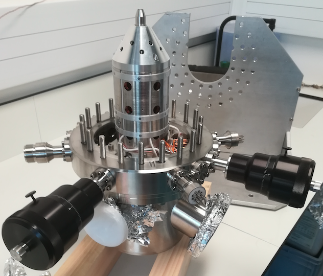
Figure 1. Spin polarized electron source developed at Laboratoire de Physique des Solides
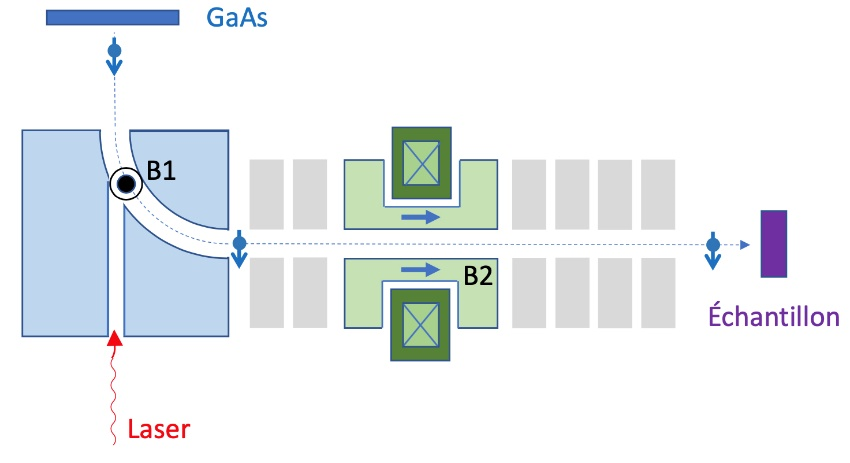
Figure 2. Schematic diagram of the electron source. A circularly polarized infrared laser (red arrow) is sent to a GaAs target, which produces polarized electrons (the blue arrow represents the spin direction) from a GaAs optical transition. The surface of the target was prepared to have a negative electron affinity, to more easily extract the electrons. Once the spin polarized electrons are produced, their orientation is completely controlled by two magnetic fields B1 and B2. The electrons are first deflected in a circular sector where the B1 field is present, which allows to choose the direction of polarization in the plane of the figure, and thus in particular to align the direction of the spins with the direction of incidence. After the circular sector, a rotator with field B2 allows to choose the polarization direction in the plane perpendicular to the incidence. By adjusting the fields B1 and B2, it is possible to obtain a polarization in an arbitrary direction (the diagram corresponds to B1 = B2 = 0).
Reference
Spin- and angle-resolved inverse photoemission setup with spin orientation independent from electron incidence angle
A F. Campos, P. Duret, S. Cabaret, T. Duden, A. Tejeda
Rev. Sci. Instrum. 93, 093904 (2022)
http://arxiv.org/abs/2110.12883
Highlights from Institut de Physique (INP)
Contact
Antonio Tejeda