| Researchers have observed the deformation and rupture of an electronic modulation present in certain crystals when subjected to an electric current, using an intense and coherent X-ray beam generated by a free-electron laser (XFEL). |
Charge transport in materials is a fundamental phenomenon for many devices, including semiconductors, superconductors, and batteries. Unfortunately, direct observation of charge movement using X-rays is not possible due to their low sensitivity to nearly free electrons. However, in systems known as Charge Density Waves (CDW), charge transport is accompanied by a deformation of the atomic lattice, which can be observed with X-rays.
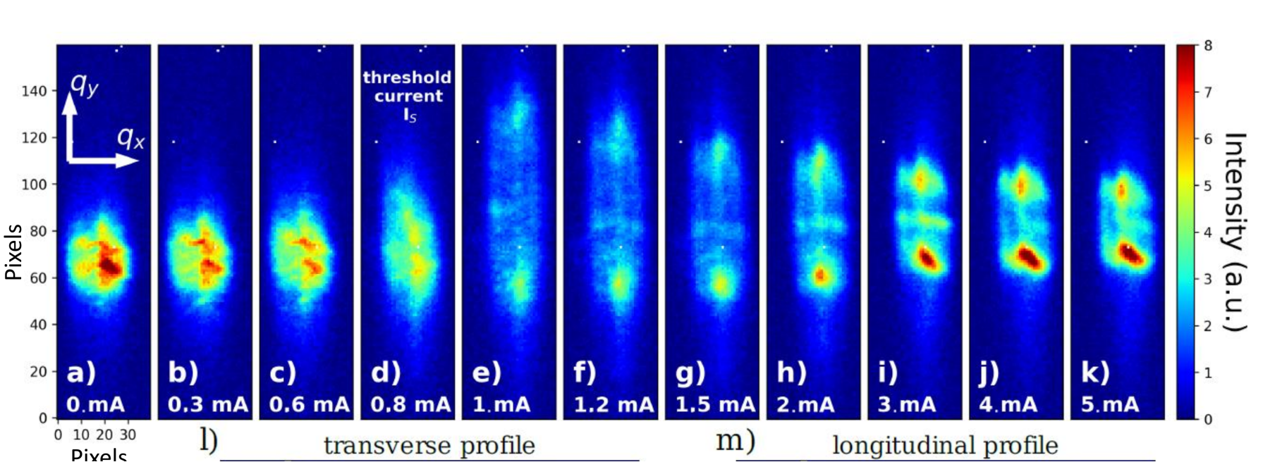
In an international collaboration involving, in particular, the Laboratoire de Physique des Solides (LPS, CNRS / Université Paris-Saclay), scientists successfully observed electronic transport in these materials by studying the behavior of the underlying atomic structure using an intense X-ray beam from an XFEL. In charge density wave systems, both electrons and the atomic structure adopt a wave-like behavior, and these two modulations are inseparable. This phase of matter is highly sensitive to various external excitations, such as temperature changes, ultrashort laser pulses, or even weak electrical currents. In the latter case, when a direct current exceeding a critical threshold is applied to the sample, an additional current appears in the crystal. This current is naturally pulsed and directly related to the behavior of the CDW. This effect is explained by the deformation of the CDW induced by the current, which ultimately breaks beyond a certain deformation threshold, periodically releasing charged topological objects that move over macroscopic distances.
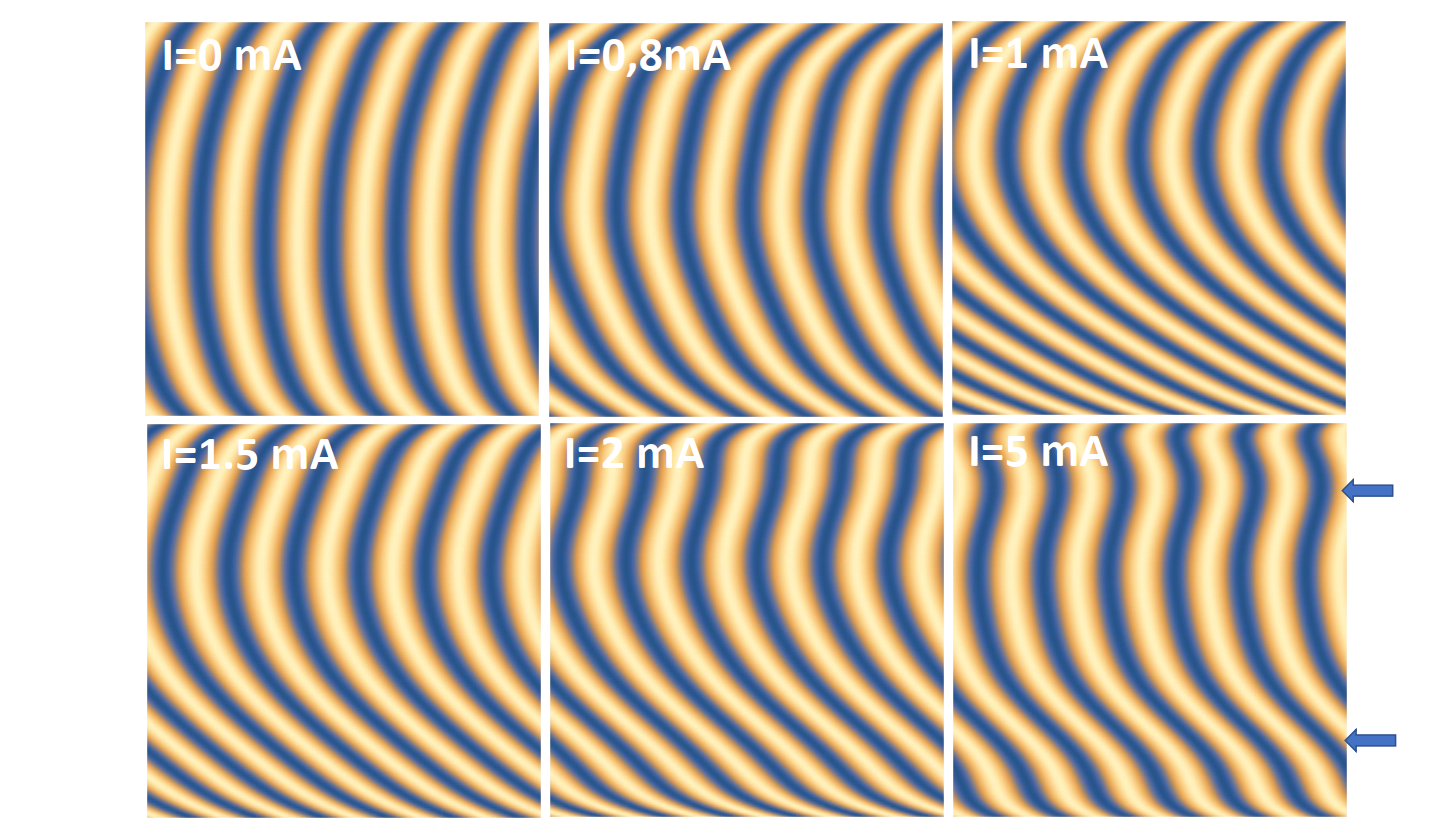
The researchers observed this phenomenon using the coherent and extended X-ray beam from the LCLS XFEL source at Stanford. The phase of the wave was deduced from diffraction patterns by applying a genetic algorithm. The CDW exhibits remarkable spatial coherence despite its nanometric periodicity. It deforms continuously from one edge to the other of the crystal, which is several tens of microns wide. Similar to a guitar string plucked at both ends and bending under an applied force, the wave bends under the influence of the current, which is trapped by the two lateral surfaces of the crystal. This shear effect increases with the current and then suddenly relaxes above the threshold current (see figure below). The wave is deformed transversely by shear but also longitudinally, akin to an accordion contracting and expanding. These two deformations—transverse and longitudinal—are closely coupled, with the relaxation of one above the threshold leading to the emergence of the other. Additionally, surface defects in the crystal act as pinning sites, preventing the wave from slipping freely.
This study highlights the capabilities of new XFEL sources, which, when combined with advanced analysis methods, open up new possibilities for observing and understanding the behavior of electronic systems. These findings are published in Science Advances.