
Linking the properties of light and the structure of a material at the nanometer scale provides valuable information for the development of optoelectronic devices. Physicists have measured for the first time the light emitted by electrons as a function of time at the nanosecond scale in an ultrafast transmission electron microscope (UTEM). This work paves the way for mapping the duration of light emission with unprecedented spatio-temporal resolution.
The excitation of a material by photons or electrons leads sometimes to the emission of light: this is the phenomenon of luminescence. The analysis of this light, including its temporal evolution, gives valuable information about the material. In the case of photon excitation, the analysis is carried out with a spatial resolution of the order of a micrometer when using an optical microscope. By using a scanning electron microscope, one reaches a nanometric spatial resolution and in this case, the excitation is produced by the electrons of the beam of the microscope: it is the phenomenon of cathodoluminescence. Moreover, if a transmission electron microscope (TEM) is used, it gives access to the atomic structure of the material. In this work, the physicists used the ultrafast transmission electron microscope (UTEM) developed at the Centre d’Élaboration de Matériaux et d’Etudes Structurales (CEMES) in Toulouse. Thanks to the insertion near the sample of a parabolic mirror with a large numerical aperture developed at the Laboratoire de Physique des Solides (LPS) in Orsay, they collected enough light to record for the first time a cathodoluminescence signal with both a spatial resolution of the order of ten nanometers and a temporal resolution of less than one nanosecond. This work is published in the journal Applied Physics Letters.
The researchers studied nanodiamond aggregates with crystal defects, called NV centers, in which a nitrogen atom coexists with a vacancy, i.e. a missing atom. While the perfect diamond is transparent, these centers are also called colored centers because of the color given by their luminescence. This luminescence is transient and its lifetime was specifically the object of the study. It was deduced from the measurement of the cathodoluminescence signal as a function of time. To carry out the experiments, the electron beam of the UTEM was pulsed with pulses of 400 femtoseconds (4.10-13 s) thanks to the excitation of the electron source of the microscope, a tungsten tip, by a femtosecond laser, and then focused on a nanodiamond sample. The main challenge the scientists faced was to distinguish signal from noise. Indeed, the current of the pulsed electron beam of the UTEM is much weaker than that of a conventional TEM, which leads to a drastic reduction of the signal emitted by the sample. For this reason, the researchers inserted a parabolic mirror with a large numerical aperture in the objective of this microscope in order to collect efficiently the emitted light (Figure 1).
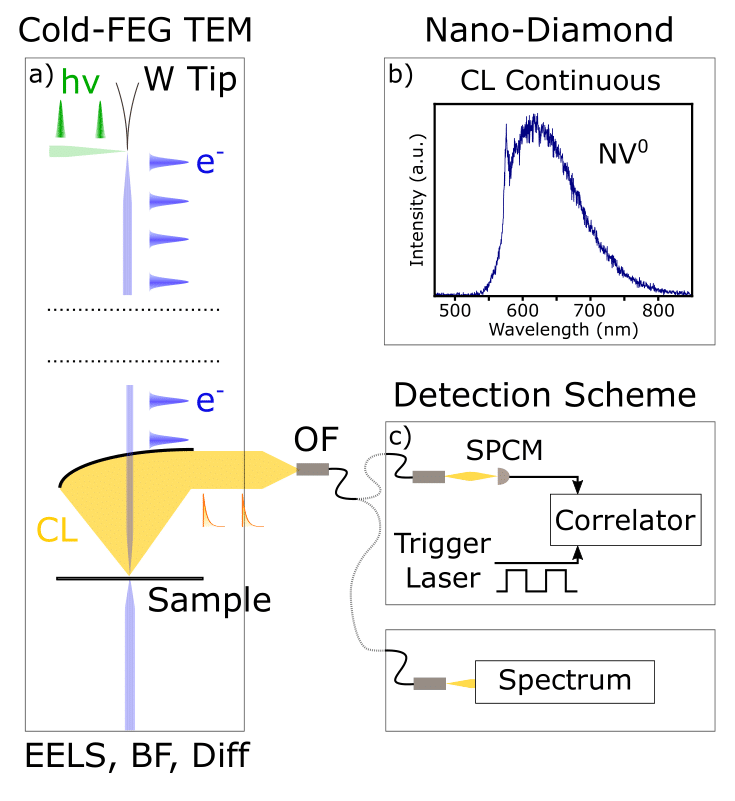
Figure 1. Schematics of the experimental set-up. a) In a modified cold-FEG Hitachi HF2000 microscope, a 2 MHz femto-second laser at 515 nm triggers the emission of femtosecond pulses of electrons from a tungsten tip. A parabolic mirror collects the cathodoluminescence from the sample. c) Thanks to an optical fiber coupled to the parabolic mirror through a lens (not shown) the light goes either to a spectrometer or to a single photon counting module (SPCM). In the later, a correlator records a histogram of the delays between excitation (trigger) and CL photon detection. Such a histogram forms a decay trace from which the lifetime of the excited state can be extracted. b) Spectrum of a diamond NV0 center, recorded in a VG510 scanning transmission electron. This spectrum was taken with a continuous beam at room temperature on the same batch of nanodiamonds used for this study. One can see the zero-phonon line at 575 nm followed by the phonon replica from 575 to 800 nm.
They have thus mapped with a spatial resolution of 12 nm the excitation lifetime of the colored centers of the nanodiamonds, of the order of 20 ns, with a temporal resolution of less than one nanosecond (Figure 2). Measuring the spatially resolved atomic structure and the temporally resolved cathodoluminescence in an integrated way in a UTEM is very promising for the study of light emission in semiconductor nanostructures: the emission yield and the charge carrier dynamics are then locally connected to the structural properties and related to parameters such as dopant concentration, stresses or electric fields. This is interesting for applications in optoelectronic devices such as photodetectors or single photon sources.
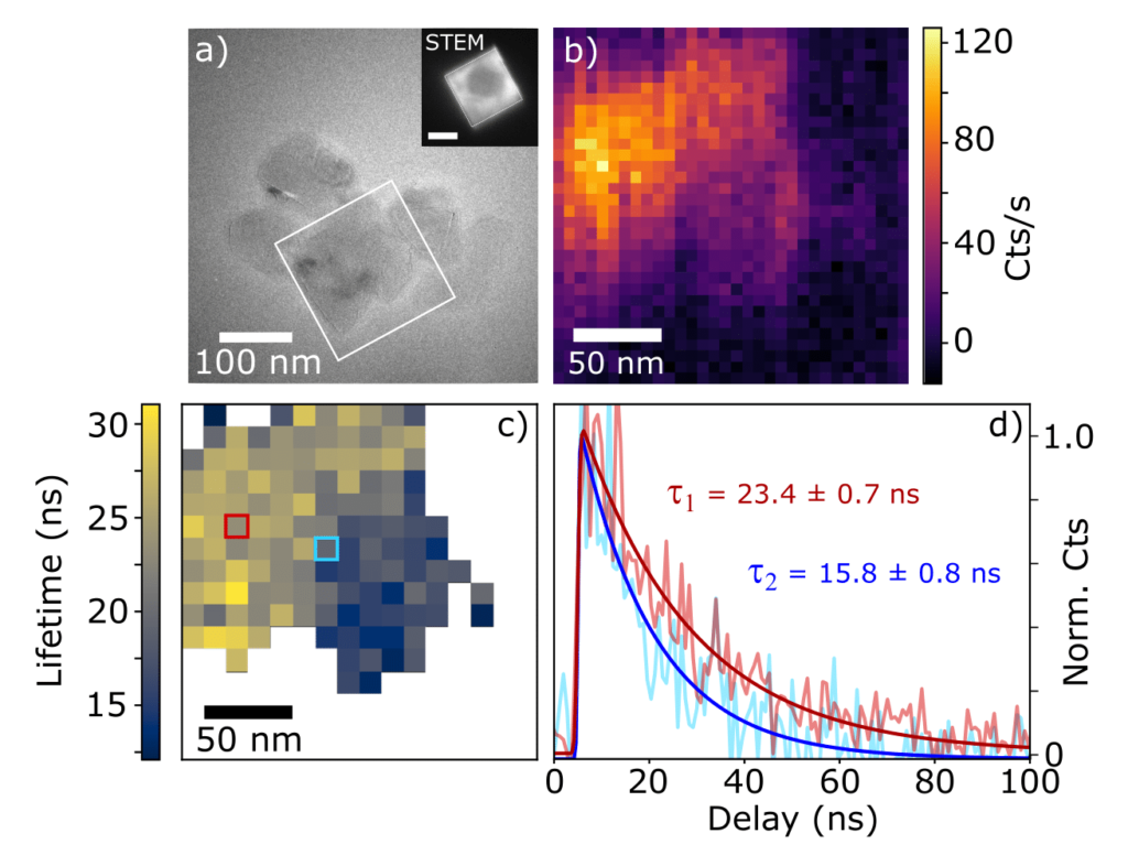
Figure 2. (a) Transmission electron microscopy image of a nanodiamond aggregate, the white square being the scanned area (inset). (b) Mapping of the cathodoluminescence emission intensity. (c) Mapping of the lifetime of the cathodoluminescence emission. (d) Time-resolved cathodoluminescence signal detected at the locations represented by the red and blue squares in (c). The noise-free lines correspond to the fit of the data for the lifetime determination.
Reference
Time-resolved cathodoluminescence in an ultrafast transmission electron microscope
S. Meuret, L. H.G. Tizei, F. Houdellier, S. Weber, Y. Auad, M. Tencé, H.-C. Chang, M. Kociak and A. Arbouet
Appl. Phys. Lett., 2021, 119, 062106
doi: 10.1063/5.0057861
CNRS-INP highlight available in french here.
Contacts
Mathieu Kociak
Luiz Tizei