
Understanding how materials absorb light on the nanometer scale is essential for applications in photonics and quantum optics. By superimposing a laser beam and an electron beam in an electron microscope with unprecedented precision, scientists have been able to study the absorption of glass and polystyrene microbeads with the utmost precision.
The optical properties of nanomaterials depend intimately on the details of their size and shape, and can vary on nanometric scales. This makes them difficult to study with conventional light microscopy. Using a scanning transmission electron microscope (STEM), atomic spatial resolutions can be achieved to image the structure of materials. Using electron energy loss spectroscopy (EELS), optical properties can be studied in parallel, with a spatial resolution of the order of tens of nanometers. However, EELS is limited to spectral resolutions ten to a thousand times too low for the study of photonic systems. Such spectral resolutions are easily obtained with lasers, but unfortunately with insufficient spatial resolution. A collaboration between the Laboratoire de Physique des Solides (LPS, CNRS / Université Paris-Saclay) and teams from Spain and Brazil has developed a light injection system in a STEM (Figure 1a), which it has adapted to a latest-generation monochromated electron microscope (CHROMATEM). The precision of this system makes it possible to optimize the injection of a laser into a STEM, and thus obtain spectral resolutions of a few hundred µeV. In this way, the technological limit predicted by the STEM-EELS system designers themselves (of the order of a few meV) has been largely exceeded.
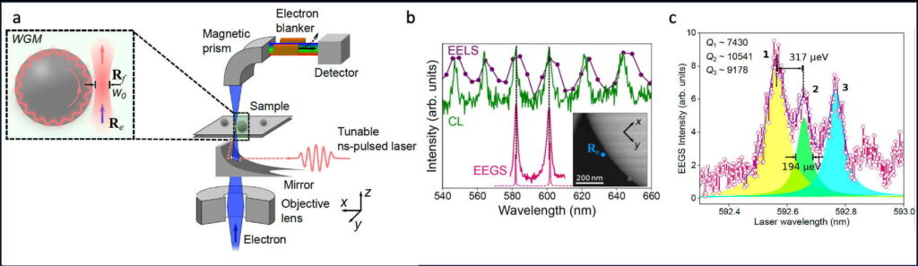
Figure 1. (a). Schematic diagram of an energy gain experiment. A fast electron (here, 200 kV) is focused on a sample at the Re point (see insert). In parallel, a laser beam is also focused at the Rf point. In this experiment, the laser beam creates a gallery mode (WGM: Whispering gallery mode). As it de-energizes, it accelerates the electron. Electron energy is measured above the sample using a magnetic prism. (b) Comparison of an electron energy loss spectrum for a silica sphere. Each peak corresponds to the energy of a mode. We can see that gain spectroscopy (EEGS) is much better resolved than electron energy loss spectroscopy (EELS, see text), or cathodoluminescence spectroscopy (CL, consisting of the light emitted by a sample after electron irradiation). C. Gain spectrum for a polystyrene sphere. We can see that very fine, partially superimposed modes are resolved. The spectral range of the spectrum corresponds to the best reported spectral resolution in EELS (electron energy loss spectroscopy).
As an application, the scientists studied silica and polystyrene microbeads in sizes ranging from 1 to 8 µm. In these beads, light is captured by internal reflection (Figure 1a, insert), giving rise to circumferentially propagating modes known as whispering gallery modes. The modes thus formed have very long lifetimes, as they cannot escape the beads, and their width at half maximum is theoretically of the order of a few µeV (to be compared with the few meV accessible in EELS). Unfortunately, it is also correlatively very difficult to inject light into them. The very precise positioning (a few hundred nanometers in all three directions) of a high numerical aperture mirror has enabled the optimal injection of a laser beam into the spheres, creating an evanescent electric field on their surface. This accelerates a beam of fast electrons (about half the speed of light) positioned at the edge of the sphere. By varying the laser energy with a precision of around ten µeV, the modes could be excited. They were then accelerating a greater number of electrons the closer the laser energy was to that of the gallery modes (Figure 1b). The energy-gain spectrum thus formed already enables modes to be resolved with a resolution two orders of magnitude better than EELS resolutions at the accelerating voltage used, and one order of magnitude better than the best EELS resolution ever reported (Figure 1c).
This is particularly interesting for a variety of applications in the fields of quantum optics and photonics. In addition, this technique could open up to many other fields of investigation such as semiconductor physics, infrared spectroscopy or quantum optics, and will require new theoretical developments to understand all its aspects. This work is published in Nature Communications.
Reference
μeV electron spectromicroscopy using free-space light
Y. Auad, E. J. C. Dias, M. Tencé, J.-D. Blazit, X. Li, L. F. Zagonel, O. Stéphan, L. H. G. Tizei, F. Javier García de Abajo, M. Kociak
Nature Communications, 2023, 14, 4442
doi: 10.1038/s41467-023-39979-0
Disponible sur arXiv
To find out more
This news was highlighted at the CNRS Institut de Physique (in French)
Contacts
Mathieu Kociak
Yves Auad